Technologies for computer aided design
The integrating of ever more complex systems requires adapted conception tools and methods. Indeed, functional and technological constraints are constantly increasing with ever smaller tolerance and shorter time-to-market. In order to meet these constraints, the typical approaches need be revised and adapted, taking complementary concepts such as increased formalism, reuse and capitalization of knowledge bases into account.
The SMH team develops compact models and multiphysics design tools dedicated to analog and mixed signal integrated systems. We develop new conception approaches dedicated to multidisciplinary systems using formal specification and hardware description languages. This is done by extending the use of applied mathematics developed for other purposes. The goal is to improve the computation speed while keeping as close as should be to the physical behavior of advanced devices.
Physical phenomena
Advanced devices as well as new fundamental devices require a thorough understanding of some specific physical phenomena. One of the team's activities is dedicated to fundamental physics modeling.
Our recent investigations have dealt with disordered layers of Si nanocrystals for floating gate applications within non-volatile memories, or random networks of carbon nanotube for chemical sensors. Currently, in collaboration with colleagues of the MaCÉPV team, we are developing a 2D model of organic solar cells.
In parallel with modeling, we also use advanced techniques for the extraction of the parameters of the model from experimental measurements.
Compact modeling

This research activity mainly focuses on the compact modeling of new fundamental devices such as ultimate transistors and also micro or nanoscale sensors developed within the team.
A large part of this activity has been dedicated to ultimate FET transistors modeling. For over 20 years now, our team has been closely working on that topic with teams from EPFL (Lausanne, Switzerland) and also URV (Tarragone, Spain). We carried out compact models for FinFET and multi-gate (featuring two, three, four gates and GAA) MOS devices. We have also been working on the modeling of junction-free nanowire-based FETs, which display promising performance in regard of future high-end IC technologies.
Sensors modeling is another part of our activity and represents a necessary step for optimizing integrated instrumentation systems. Within that framework we developed models for magnetic sensors based on the Hall effect (HHD and VHD) and charge deflection (CHOPFET).
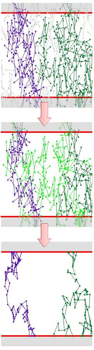
More recently we started new research projects on the modeling of chemical sensors. We have been specifically studying two kinds of sensors, carbon nanotube FET (CNTFET) on one hand and ion sensitive FET (ISFET) on the other. Both devices can be potentially functionalized in order to be used as biosensors.


Related projects
The principal projects related to the compact modeling activities are:
- FP7 COMON, ended 2012, "Modeling of multi-gate SOI transistors"
- ANR XYZ-IRM and SATT project, "Development of a dedicated system for active minimally-invasive surgery tools tracking in MRI environment"
- ANR CAPTEX, 2010-2013, "Modeling of CNTFET-based explosive gas sensors and development of their dedicated fully integrated conditioning electronics"
- industrial project in collaboration with BURKERT company, "Virtual prototyping of Lab-on-Chip (LoC) for pollutant detection"


High-level multiphysics modeling and simulation tools

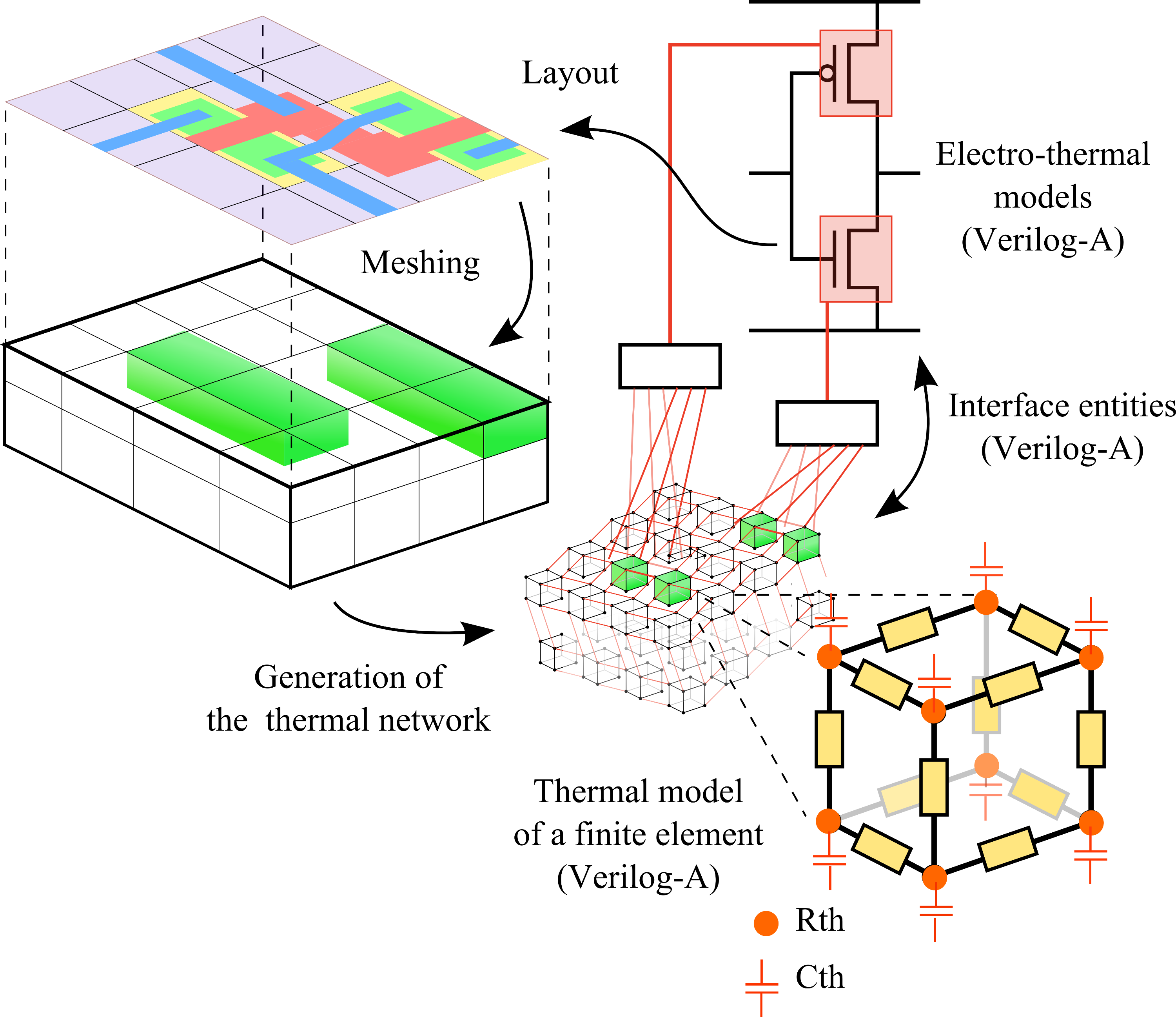
In order to be able to meet the ever growing requirements in IT and mobile devices, the IC manufacturers gradually turn to 3D integration, which consists in stacking chips thus forming complex single-package systems. Such an approach allows to look into the opportunity of new solutions to stick to Moore's law or even achieve "more than Moore" performance, but it also come with several shortcomings. In particular, evacuating the heat produced within an integrated chip is particularly difficult and induces an increase of the average operating temperature and also hotter spots. Besides being responsible for higher power consumption, these thermal issues also induce additional mechanical constraints due to material expansion and have overall negative impact on chips' reliability.
As it is the aging mechanisms that occur in integrated circuits (electromigration NBTI,...) are all the more important with high temperature. In order to minimize these harmful effects, it has now become essential to take thermal and mechanical characteristics into consideration at the early stage of IC development.
In that context, since 2009 we have been working on the development of a multiphysics (i.e. electrothermal and mechanical) simulator, embedded into one of industry's standard CAD tool, namely CADENCE®. Now, our team is in possession of an experimentally validated operational tool dedicated to simulating electrothermal and mechanical behavior in the IC engineering flow. This enables high accuracy circuit behavior simulation and should ultimately allow accurate forecasting of an integrated system's lifetime, i.e. prior to failure.


Related projects
The principal projects related to the compact modeling activities are:
- ANR 3D-IDEAS, ended 2012, "Integration and 3D conception technology for imaging systems and applications"


Tools for synthetic biology
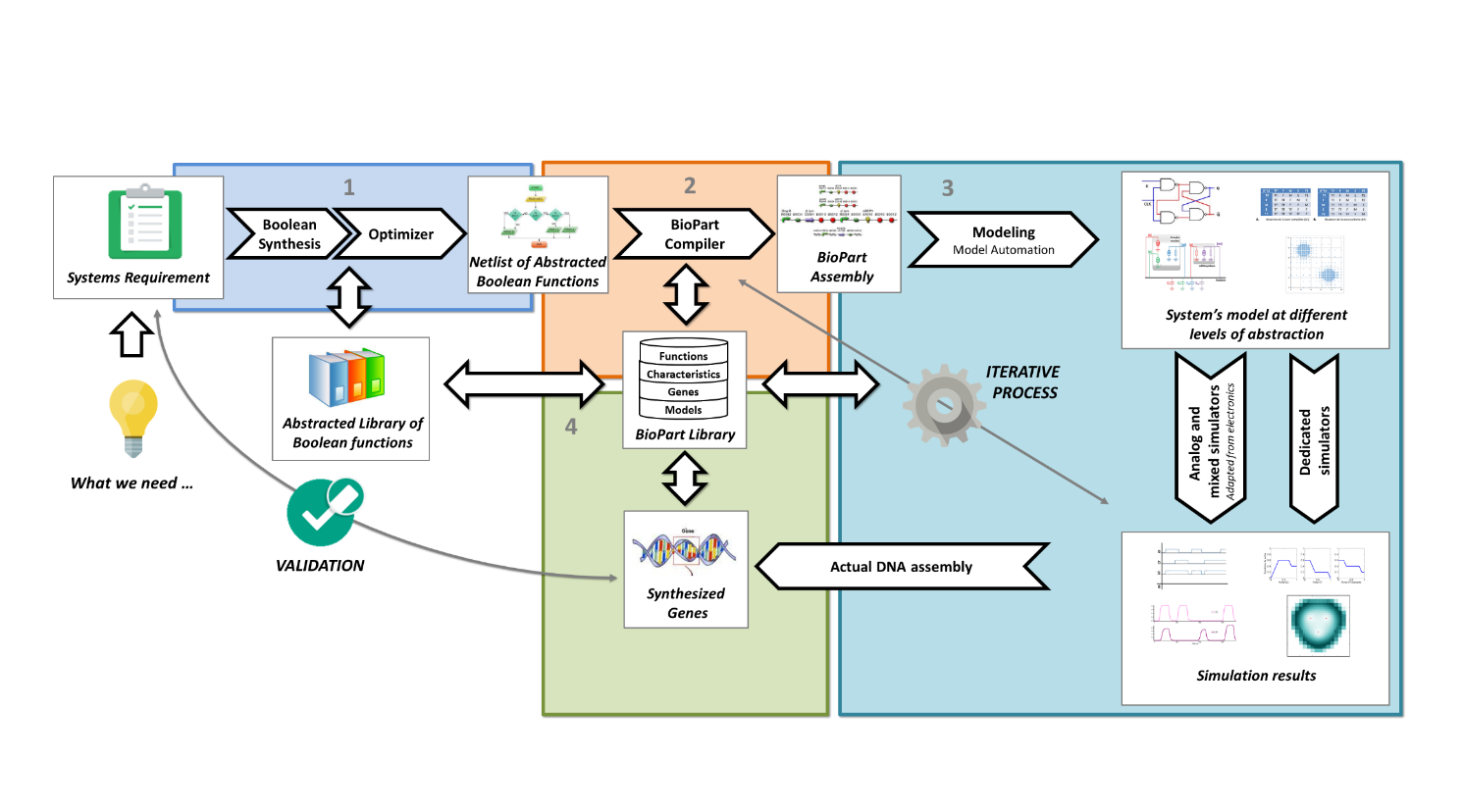
The large base of knowledge in the area of technology for integrated circuits design can be applied to other fields and on media that differ from semiconductors such as synthetic biology. This is a new area where biotechnologies meet semi-conductor and computer sciences. The goal is to investigate the possibilities to adapt IC Computer Aided Design (CAD) tools for biological systems design. This could help engineers in biotechnology to create new biological functions by assembling appropriate elementary blocks (i.e. DNA sequences) as in the synthesis process of digital integrated ICs. One activity of the SMH team precisely consists in identifying and make use of the similarities between these two fields. This activity is a part of the "Technologies for computer aided design" activities since it addresses the modeling of elementary blocks and the development of CAD tools (components library, biological synthesizer, dedicated simulator, optimizer ...).
The figure below shows the 4 main steps of a system's design flow using CAD tools, i.e. 1) high-level automatic synthesis, 2) elementary functions library low-level synthesis, 3) virtual prototyping (modeling, simulation and optimization) and 4) final assembly for manufacturing and test purpose. Our team mainly addresses steps 1 to 3. For step 1, we proposed to adapt an open-source logical synthesizer in order to perform elegant high-level synthesis. For step 2, we have been investigating the potential of evolutionary algorithms. For step 3, we developed various VHDL-AMS models and formalisms able to describe biological systems. This leads our team to develop a tool that can generate biological models using generic bond description between a macromolecule and a ligand.
The last step in this design flow is the validation of the built bio-system. We are currently investigating some new leads to perform the characterization of the system by measuring the fluorescence (i.e. the response of the system) on a modular 3D printed lab-on-chip.
